Nanosecond Nirvana: The Art of Focusing a 20-Micron Metal Sphere in a
The precision demanded by contemporary semiconductor fabrication is a perpetual war against entropy. The primary obstacle is a droplet of tin—a metallic sphere a mere 20 microns in diameter that must be steered with absolute fidelity into the focal point of a laser beam. Should the droplet deviate by even a few micrometers, the entire 250-watt energy payload dissipates into futility, subjecting the system to a violent thermal shock. This is no abstraction; it is an engineering crucible where one must master the fluid dynamics of molten metal within a vacuum, where a pressure of 10^-9 mbar forces molecules into behavior of profound unpredictability. Each droplet, hurtling at 50 meters per second, represents a potential catastrophe if its trajectory is not governed to the sub-nanometer scale.
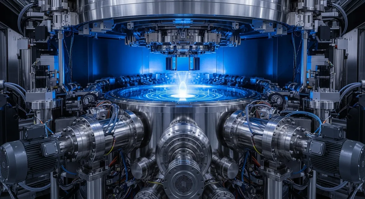
This volatile matter is contained within a 2.5-meter-diameter SS304 stainless steel chamber. Its walls are far more than a passive shell; they are a structural fortress designed to withstand external atmospheric pressure fluctuations that would otherwise warp the optical axis. Here, the metal acts as an insulator between the chaotic external environment and the sterile interior. When the plasma-generation explosion occurs within, the SS304 steel absorbs the acoustic waves, preventing them from manifesting as mechanical vibration. It is a material chosen for its corrosion resistance and thermal expansion stability, maintaining vacuum integrity even when temperature gradients spike by hundreds of degrees per millisecond.
The transmutation of the tin droplet into plasma is an act of thermodynamic violence. When the CO2 laser discharges a 20-millijoule pulse, the tin undergoes an instantaneous phase transition from liquid to ionized gas plasma. In this process, temperatures soar to millions of degrees, and the released energy becomes the source of extreme ultraviolet (EUV) radiation at a wavelength of 13.5 nanometers. This is no gentle luminescence, but an intense flux of radiation that physically erodes everything in its path. Materials here endure extreme bombardment, and tin ions, if not properly diverted by magnetic fields, deposit themselves upon optical surfaces, rapidly annihilating their reflectivity.
The light flux is governed by multilayer molybdenum and silicon mirrors. Each of the forty layers is deposited with atomic precision to ensure the constructive interference necessary to reflect the 13.5-nanometer wavelength. Molybdenum serves as the structural backbone, resisting the thermal expansion induced by absorbed energy, while the silicon layers create the optical barrier. This structure functions as a molecular filter, rejecting all extraneous radiation to leave only a pure, focused stream of photons for the lithographic process.
The surface quality of these mirrors is such that any deviation from ideal geometry exceeding 0.5 nanometers compromises the entire optical path. This necessitates a base of absolute inertness. Consequently, the entire optical system is mounted upon a massive granite block. Granite, possessing an exceptionally low coefficient of thermal expansion, acts as a vibration dampener. Its mass and density absorb both the turbulence of the processor cooling systems and the seismic noise of the building, allowing the optics to remain stable even as the environment around them trembles.
The control system, comprised of 500,000 lines of code, executes constant, iterative corrections. Sensors measuring temperature with 0.1-degree precision relay data to a processor that, within microseconds, adjusts the laser-focusing lenses. PID algorithms here are not mere theory; they are real-time tension management, where each piezoelectric actuator performs microscopic movements to compensate for material expansion. It is a continuous feedback loop in which software becomes a physical component of the system, ensuring that 5-nanometer lines are etched without a single deviation.
The operation of the entire system relies upon turbomolecular pumps that continuously evacuate gas molecules from the chamber, ensuring the vacuum remains free of obstacles to the photon flux. Each pump bearing rotates at 60,000 revolutions per minute, generating heat that must be actively dissipated through liquid nitrogen cooling circuits. This infrastructure is the invisible anatomy of the machine; without it, the plasma source would extinguish within seconds, choked by residual gases.
This apparatus represents the frontier of engineering, where materials physics and digital logic collide. There is no room for chance—every component, from the SS304 steel chamber to the molybdenum mirrors, is engineered to withstand conditions that are impossible in the natural world. It is a process where nanometric precision becomes mundane, and the laws of physics are not obstacles, but the very tools with which we write our digital future. Every chip that emerges from this system is proof that human-built infrastructure can transcend the chaos of the natural order.
The technologies of the future demand even greater precision. As we transition to structures smaller than 5 nanometers, current methodologies will require a total reassessment. Materials science must yield even more resilient mirrors, and control algorithms must evolve into processors capable of reacting to fluctuations before they occur. It is an endless engineering odyssey, where every technical refinement is merely the prologue to a new challenge, and our capacity to comprehend and manipulate physics remains the only limiting factor.