Mechanical Harmony: The Resonant Bond of Silicon Nitride and Atomic Forces
The silicon nitride cantilever at the heart of an atomic force microscope is far more than a passive component; it is a dynamic mechanical system whose behavior is dictated by the precise ratio of stiffness to mass within a plate 0.5 to 1.5 micrometers thick. Oscillating at a resonant frequency of 400 kHz, the material’s fabric undergoes relentless cycles of tension and compression, constrained by a Young’s modulus of 310 GPa. In this frequency regime, every molecular bond acts as an inertial brake, and the internal matrix must endure immense dynamic loads to stave off structural fatigue—a failure that would manifest as an unpredictable, drifting resonance.
Thermal fluctuation, manifesting as Brownian motion, serves as the fundamental source of entropy that constrains the cantilever’s sensitivity. As ambient heat induces stochastic vibrations in surface atoms, the cantilever absorbs this energy, relying on its spring constant—ranging from 0.01 to 100 N/m—as the sole barrier preventing this noise from drowning out the signal. Each molecular node of the silicon nitride acts as a phonon scatterer, yet even at optimal material density, residual thermal energy creates a persistent, stochastic background that engineers must excise through the application of sophisticated digital algorithms.
The interaction between the probe tip and the sample surface induces a localized pressure concentration that, at a tip radius of 5 to 10 nanometers, exceeds the 10 GPa threshold. This mechanical stress forces the crystalline structure at the contact point to adapt to extreme conditions, where Van der Waals forces emerge as the dominant mechanism of interaction. The material’s resistance to deformation in this zone is critical; any shift in tip geometry resulting from atomic diffusion immediately alters the measurement space, introducing systemic error.
The piezoelectric scanner, composed of lead zirconate titanate, functions as a high-precision transducer, converting a 1000 V electrical potential into mechanical displacement. Within this ceramic matrix, the movement of domain walls generates not only the intended motion but also parasitic capacitance, which becomes a primary source of electrical noise. As voltage is modulated with an accuracy of ±0.1 nanometers, hysteresis energy accumulates within the material, necessitating dissipation through cyclic polarization to prevent the non-linear shifts that distort the scanning trajectory.
The 10-millimeter-thick base of anodized Al6061-T6 aluminum acts as an inertial damper, isolating the entire optical and mechanical assembly from external vibrations. Yet, even such a massive structure is not entirely inert; it remains susceptible to acoustic disturbances that resonate at the base’s natural frequencies. To achieve maximum stability, the plate surface is machined to a flatness of ±0.1 micrometers, minimizing mechanical "rebound" during scanning and maintaining a stable reference point even under significant loads.
The integration of an Invar alloy into the base structure is a calculated response to the problem of thermal expansion, which, if left unchecked, would trigger microscopic shifts in the measurement axis. Composed of 36 percent nickel and 64 percent iron, this alloy possesses an exceptionally low coefficient of expansion, maintaining dimensional stability even as ambient temperatures fluctuate by mere fractions of a degree. This ensures the device’s entire fabric remains in a static geometric state, preventing thermodynamic expansion from bleeding into nanometric-scale measurements.
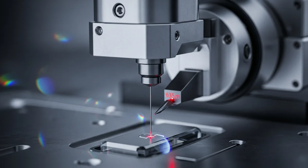
The laser diode, emitting light at 635 nanometers, creates an optical lever that allows for the observation of cantilever displacements with a sensitivity of 10⁻⁶ to 10⁻⁸ meters per volt. The photon flux reflecting off the rear of the cantilever becomes a carrier of information, its amplitude directly proportional to the mechanical deflection. However, this optical circuit is plagued by photonic shot noise—a consequence of the statistical variance in photon arrival times—requiring the detector to possess high quantum efficiency to distinguish the true signal from random light pulses.
The digital signal processor, governing PID algorithms, executes real-time corrections essential for maintaining a constant force between the tip and the surface. This process relies on a high-speed feedback loop where every fraction of a millisecond is dedicated to minimizing error; however, the processor’s finite clock speed and the ADC converter’s sampling rate impose a theoretical limit, preventing the total elimination of dynamic errors encountered when scanning highly irregular surfaces.
Quantum noise, arising from electron tunneling at the interfaces of piezoelectric elements, remains one of the most intractable problems limiting measurement resolution. As voltage approaches zero, the electron flow becomes discrete, introducing additional uncertainty into the system’s positioning. This parasitic capacitance, coupled with the noise floor of the control electronics, establishes a "measurement floor" that can only be breached through cryogenic cooling, which suppresses the thermal activity of the electrons.
Ultimately, the limits of atomic force microscopy are defined not merely by engineering precision, but by the physical nature of material interaction. As the tip approaches the surface, Van der Waals forces and electrostatic attraction entwine into a complex field that is difficult to deconvolve into discrete components. The primary engineering bottleneck remains the contact area between the tip and the surface: reducing the tip radius to the atomic scale increases the uncertainty of interaction forces caused by the variable arrangement of surface atoms, leaving even an ideally balanced system to face the fundamental paradox of balancing measurement accuracy against physical perturbation.