The Volatile Molecular Veil: Unforeseen Consequences of Residual Gas Adsorption in Tung
Within the vacuum chamber, where pressure plummets to the 10⁻⁹ mbar threshold, an unsettling phenomenon emerges: the residual adsorption of gases onto the tungsten-rhenium alloy probe tip precipitates an unwanted molecular "sheath." Though this layer is a mere few atoms thick, it fundamentally alters the probe’s work function, transmuting a precision instrument into a volatile signal generator. The tip’s geometry—a 90 percent tungsten and 10 percent rhenium matrix—surrenders its 10–20 nanometer radius accuracy to this contamination, inducing a "ghosting" effect where the scanned surface appears draped in spectral, duplicated topographies.
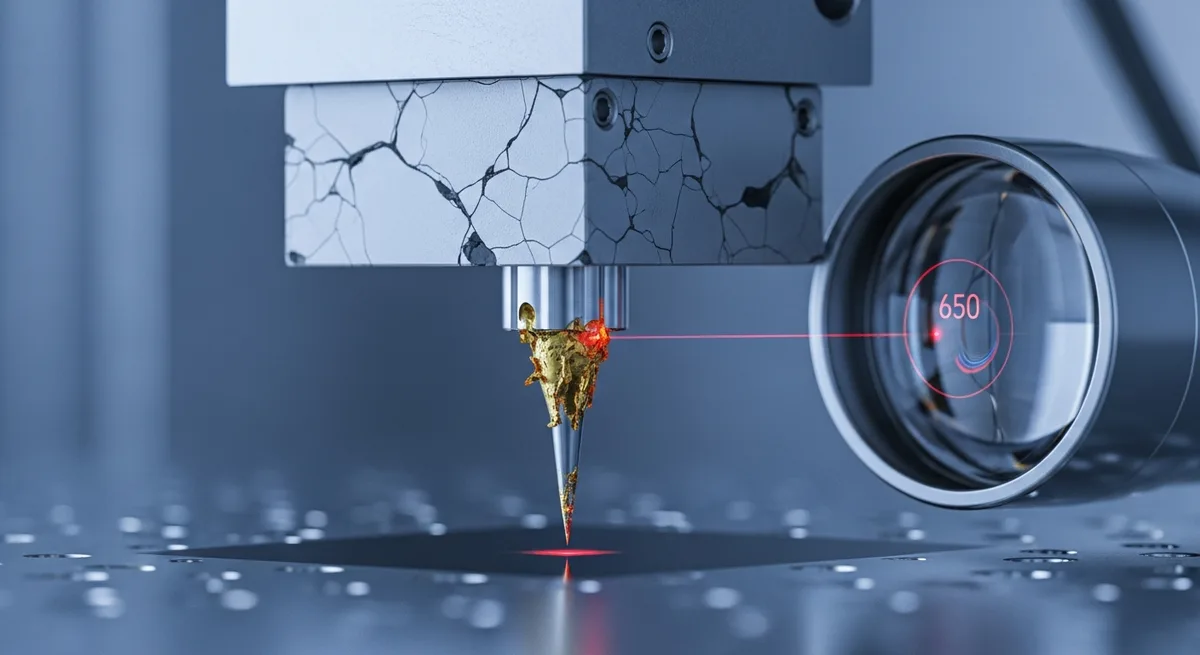
The etching process of the tungsten alloy wire, requiring a potential of 1–10 volts and a current of 1–10 microamperes, occasionally seeds microstructural defects at the apex. Subjected to the equivalent of 3400–3500 degrees Celsius melting points, these defects manifest as localized hot zones; despite the structural resilience of a 400–500 GPa Young’s modulus, they trigger acute thermal drift. When the 10–50 nanometer gold coating, deposited at 10–50 watts of power, begins to delaminate under the stress of uneven thermal expansion, the probe severs its electrical contact with the surface, precipitating an instantaneous current spike capable of liquefying the specimen itself.
The silicon cantilever, serving as the mechanical transducer, exhibits an indirect dependence on a spring constant of 0.1–10 N/m. When this element—100–200 micrometers in length and 1–2 micrometers in thickness—encounters a resonant frequency exceeding 100 kHz, a "jumping" effect occurs. The beam loses its tether to the surface and descends into chaotic vibration, generating reflection errors within the 10–50 nanometer aluminum layer that the optical system interprets not as topographical reality, but as a persistent, incoherent hiss of noise.
The 99.99 percent pure silicon fabric, sculpted via deep reactive-ion etching to a width of 20–50 micrometers, is prone to fatigue fractures if the PID controller reacts with excessive aggression to surface irregularities. As the 10–50 watt aluminum coating overheats, its reflection coefficient fluctuates, inducing deviations in the laser beam’s focus. This forces the lenses—possessing a numerical aperture of 0.5–1.0—into a state of perpetual adjustment, yet the optical axis invariably lags behind the mechanical deformation, causing the photodetector signal to forfeit the integrity of its 10–100 kHz frequency band.
The PZT material block, measuring 10x10x2 millimeters, acts as the system’s primary engine of instability due to its 500–600 pC/N coefficient. When the voltage supplied by the 10–100x gain amplifier shifts abruptly, the piezoelectric element suffers from hysteresis, accompanied by internal mechanical stress. At the 350–400 degrees Celsius Curie temperature limit, this stress propagates micro-cracks throughout the ceramic matrix, skewing the probe’s three-axis trajectory by 10 to 100 micrometers horizontally and 1–10 micrometers vertically.
As the 635–650 nanometer laser reflects off the cantilever’s dorsal side, the photodetector—with a responsivity of 0.5–1.0 A/W—captures not only surface data but also parasitic optical interference. These interferences, born from the imperfections of the 10–20 millimeter focal length lenses, conjure phantom signals that the DSP processor, operating at a 100–1000 MHz clock frequency, misinterprets as non-existent topographical "peaks." This triggers an over-correction by the PID controller, forcing the entire system to oscillate violently around its point of equilibrium.
The digital signal processor, executing C++ algorithms, attempts to dampen these oscillations, yet the 10–100x amplified signal frequently breaches the dynamic range of the analog-to-digital converter. As the DSP attempts to excise this noise via low-pass filters, critical information regarding the atomic structure of the surface is discarded. Consequently, the 0.1–1 nanometer resolution becomes an unreachable horizon, leaving behind only artifacts of computational error that bear no relation to the material’s true topography.
Temperature fluctuations of ±0.1 degrees, while seemingly negligible, induce microscopic shifts in the 10⁻⁹ mbar vacuum seals. These perturbations, though imperceptible at a macroscopic scale, trigger a mechanical "settling" of the system that the PZT scanner attempts to compensate for, only to reach its physical limit of 100 micrometers of horizontal travel. At this juncture, the system stalls; the probe, no longer capable of raster motion, begins to "plow" the surface, inflicting irreversible damage upon both the specimen and the tungsten tip itself.
Ultimately, the fundamental engineering barrier is not the sensitivity of the probe, but the dissonance between information processing speed and mechanical response. Although the DSP processor operates at 1000 MHz, the piezoelectric material’s reaction time is shackled by its own internal structural inertia. When the scanning speed exceeds 10 kHz, the piezoelectric block is no longer capable of faithfully replicating the impulses dispatched by the DSP, resulting in a phase shift that renders the entire measurement process a physical paradox: the more data the system attempts to harvest per unit of time, the less reliable each measured coordinate becomes.