13,5 nm fotonų generavimas jonizuojant greitaeigius alavo lašus
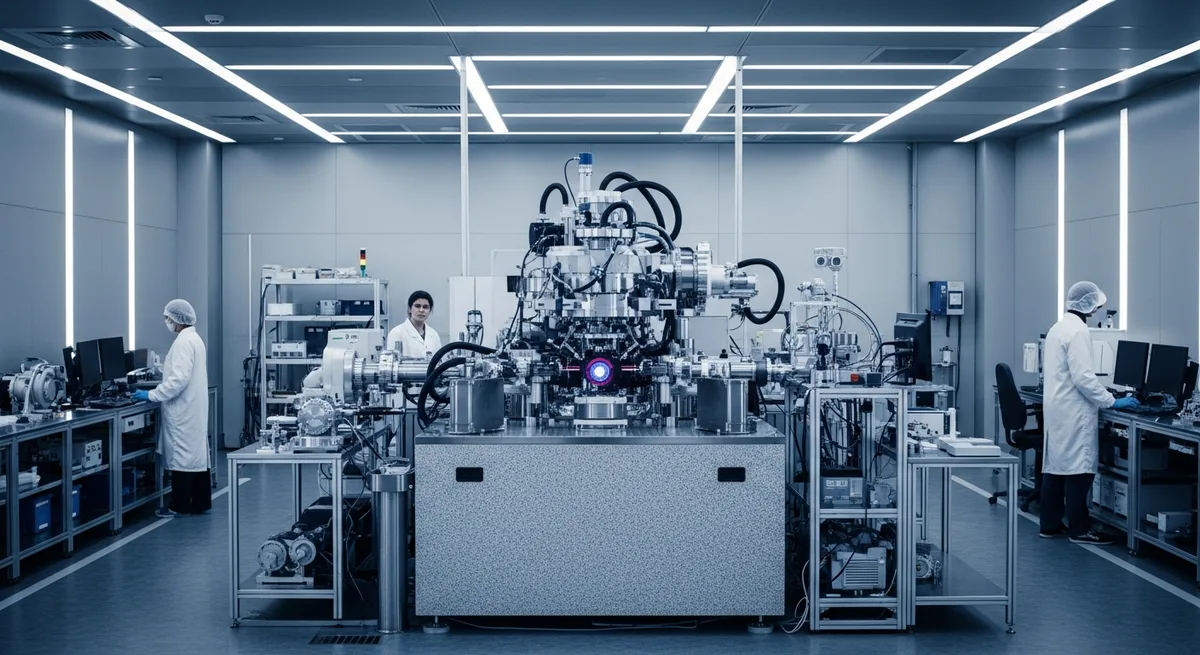
The Extreme Ultraviolet (EUV) lithography system is no mere abstraction; it is an engineering ultimatum issued to the fundamental recalcitrance of matter. When a laser, pulsing with 50 kilowatts of raw power, strikes a droplet of molten tin, the result is not a "dance," but an aggressive physical collision. The tin, hurtling at 10 meters per second, is ionized in a heartbeat. This violent transformation yields more than just 13.5-nanometer photons; it generates a spray of high-kinetic-energy tin ions. These ions are the system’s primary antagonist, scattering in every direction to bombard optical surfaces and physically displace atoms from their lattice positions. This is not metaphorical wear; it is atomic-level erosion, a degradation that engineers must arrest with hydrogen flows, crafting a protective gas barrier before the very first mirror.
Each of the six primary mirrors is forged from glass-ceramic with an ultra-low coefficient of thermal expansion. In this environment, a temperature fluctuation of even a few hundredths of a degree induces mechanical stress sufficient to distort the entire optical axis beyond permissible tolerances. The mirror surfaces are coated in molybdenum and silicon layers, their periodicity tuned precisely to the 13.5-nanometer wavelength. This internal matrix functions as a selective filter, yet each layer must endure not only the photon flux but also a relentless thermal cycle, where energy absorption triggers microscopic pulses of expansion. Were the material’s fabric less precise, these pulses would, in short order, render the mirror a useless shard of glass.
The mirror substrate itself represents the absolute frontier of engineering. It must possess extreme rigidity to withstand 70 gigapascals of mechanical stress without a hint of deformation, ensuring the optical path remains immutable even under peak load. Yet, this hardness demands a price: brittleness. Every stage of the fabrication process for this structural frame is a gamble; should a microscopic fissure emerge during surface polishing, the mirror will fail to survive the thermal load and shatter. It is a material whose properties align more closely with diamond than with conventional glass.
Beneath the optical assembly, the granite base serves a singular, vital function: the absorption of vibration. This 1.2-meter-diameter granite disc is no mere slab of stone; it is an inertial damper. The piezoelectric actuators that manipulate the silicon wafer generate microscopic oscillations, and the granite’s mass and internal crystalline structure act as a filter, dissipating these tremors. Should the wafer’s position shift by even five nanometers, the entire lithographic process would be compromised. Here, the granite stands as the only stable anchor in a chaotic environment governed by a vacuum pressure of 10^-6 pascals.
The vacuum chamber is a theater of perpetual engineering warfare. Turbomolecular pumps spin at 60,000 revolutions per minute, scavenging every stray molecule capable of absorbing EUV radiation. In this vacuum, materials behave with alien unpredictability: metals outgas, and lubricants become contaminants. Consequently, all internal junctions are treated to ensure maximum surface inertness. This is no empty void; it is a meticulously curated environment where the presence of even a handful of gas molecules could deflect the light’s trajectory, unraveling the atomic network being etched onto the silicon wafer.
The algorithmic control governing this complex is more than software; it is a real-time computational nervous system monitoring every piezoelectric twitch. Sensors encircling the mirrors measure distances with picometer precision. If the plasma source generates a pulse even slightly off-center, the algorithm recalibrates the entire optical chain within microseconds. It is a constant, reflexive response to the volatile conditions inherent in the process itself—a machine that perpetually learns its own flaws, attempting to compensate for them before they manifest as catastrophic errors.
Positioning the silicon wafer is an engineering tightrope walk. The wafer must be aligned beneath lenses with a numerical aperture of 0.33. This aperture defines the light-gathering capacity and the ability to focus energy into a single point; the higher the value, the smaller the transistors that can be rendered. Yet, with this power comes the rising specter of optical aberration. Each lens and mirror must compensate for the errors of its neighbor in an iterative process where engineers balance the razor’s edge between optical power and systemic physical stability.
When we speak of five-nanometer transistors, we are discussing structures approaching atomic dimensions, where the laws of classical physics begin to fray. Electrons begin to tunnel through insulating layers. This system is designed specifically to harness this chaos. By utilizing a 13.5-nanometer wavelength, we possess a tool precise enough to engrave structures where these quantum effects are not merely managed, but anticipated. This is not mere manufacturing; it is the manipulation of matter at the subatomic level.
The SS304 stainless steel used for the chamber housing serves a specific purpose: it is robust enough to withstand atmospheric pressure under vacuum while maintaining an exceptionally low outgassing coefficient. This is critical, as any impurity in the system could settle upon the optics. An internal aluminum coating further suppresses particle generation. Every component, every bolt, is engineered to preserve this sanctity of cleanliness. It is an engineering philosophy where purity is as vital as mechanical strength.
The modern photolithography system is a technical monument to our civilization. It functions as an invisible engine, rewriting the boundaries of our potential. It is not merely a machine that produces processors; it is a machine that dictates the potency of artificial intelligence, the limits of our computational reach, and the depth of our understanding of the universe. Every component, from the tin-droplet generator to the piezoelectric actuators, is tuned to act as a singular entity where the laws of physics are not merely observed, but actively leveraged.
The process itself is a relentless challenge to entropy. Each component battles environmental interference to maintain its form and function. It is a battlefield where we prevail through precision. By ensuring that every nanometer remains in its designated place, we guarantee that our technological trajectory remains unbroken. The devices of tomorrow will be more powerful not by miracle, but because we have learned to command matter with a precision that seemed impossible only decades ago.
This system stands as proof that the human intellect can master even the most extreme physical phenomena. When 20,000-Kelvin plasma is transmuted into light, and that light into a microchip, we witness more than technology—we see human will embodied in steel and granite. Every detail serves a purpose; every action is calculated with staggering accuracy. It is a silent, patient process of creation, where every step yields greater performance and heightened efficiency.
We inhabit an era where technology grows increasingly complex and woven into the fabric of our daily lives. The EUVL system serves as the foundation upon which our entire digital infrastructure rests. Though it remains cloistered and inaccessible, its influence is universal. Every smartphone, every server, relies upon this technology. It is a triumph of engineering, demonstrating how far we can reach when we fuse scientific knowledge with practical application, altering the world from within, atom by atom.
Ultimately, the EUVL system is a technical monument to our civilization. It is a machine that does more than manufacture processors; it shapes the trajectory of our world. It demands our respect as a reflection of our greatest achievements. It is a technological miracle, quietly and patiently crafting a future where computational power becomes boundless. We are both the observers and the architects of this process, perpetually pushing the limits of the possible and proving that even the most complex laws of physics can be brought to heel.
Within the vacuum chamber, the silence is so profound that only the pulsing of electronics remains. Each laser pulse and each mirror tilt is a fragment of a larger tableau, where every nanometer signifies new possibility. This system is the guarantor of our progress, cementing our capacity to manipulate matter. This is the essence of engineering: to transmute chaos into order, and energy into information, creating that which only yesterday seemed impossible.
The complexity of the system is staggering, yet it is precisely this complexity that allows us to achieve the impossible. Every component and process is meticulously considered to ensure stability and precision. It is a triumph of engineering, showing how far we can go when we unite scientific knowledge with practical application. We are changing the world from within, atom by atom, nanometer by nanometer, ensuring that our technological progress never falters.
This system is a constant challenge to entropy. Each element fights against environmental influence, striving to maintain its form and function. It is a battlefield where we win not by force, but by precision. By ensuring that our technological progress continues, the devices of tomorrow will be even more powerful than those of today. This is the promise of EUVL—to create a future where the impossible becomes reality. We are on this path, and every step is essential.
In conclusion, it is safe to assert that this system is a technical monument to our civilization. It is a machine that not only produces processors but shapes the direction of our world. It is proof that we are capable of mastering the deepest laws of physics and harnessing them for our benefit. This technology demands respect as a reflection of our greatest achievements—a technological miracle, quietly and patiently creating our future.