Taming Entropy: A Quantum Leap in Photonic Architecture
We often labor under the misconception that engineering is merely the imposition of form upon matter, yet the reality is far more visceral—a perpetual, grinding war against entropy, which seeks to dismantle every architecture of order we dare to construct. Within the laboratories of modern photonic architecture, we no longer merely build devices; we attempt to domesticate the chaos that erupts at the threshold of quantum tunneling. When a signal, transmitted in intervals of 10–100 picoseconds, suddenly sheds its coherence, we are not witnessing a mechanical failure—we are confronting physics’ refusal to submit to our logic. It is the precise moment when a photon, as if startled by the prospect of its own liberty, chooses to abandon the silicon dioxide channel and vanish beyond the confines of its intended path.
Every element of the 200–300 nanometer lattice is calculated to contain this inherent unpredictability, yet the physical resistance of the material is far more than a mere numerical value. When a field of 50–100 W power bombards the SiO2 matrix, we can sense the atomic lattice straining under the load. This is no mere metaphor for tectonic shifting; it is a cold, mathematically precise tension felt by every individual chemical bond. Could you hear the process, it would not be the groaning of metal, but the sharp, crystalline “crackle” of structural fatigue as ions, under 10–50 mTorr of pressure, displace atoms to leave behind only what is essential for signal integrity.
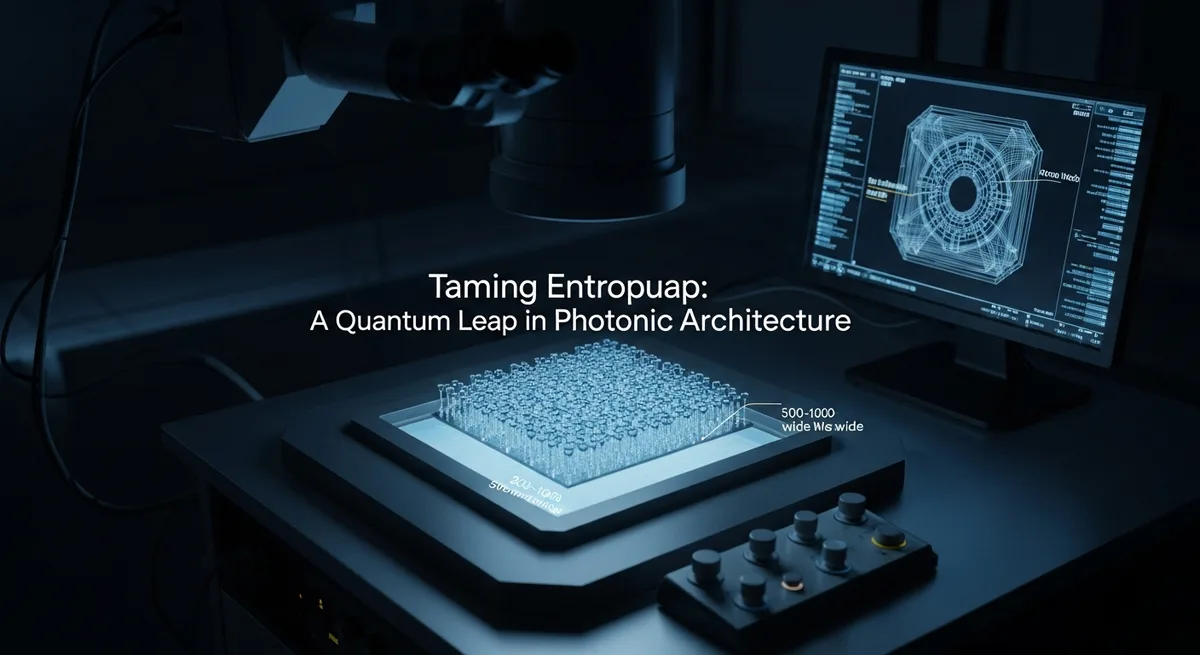
Titanium dioxide inserts, with their refractive index of 2.45, play a critical role in this delicate equilibrium. They are not the “brains” of the operation; they are more akin to navigational beacons in a tempestuous sea. When the light flux reaches the 500–1000 nanometer-wide optical highway, it must preserve its wave phase despite ambient temperature fluctuations or microscopic material defects. Each such defect acts as a point of energy leakage, where a consumption of 10–100 fJ is no longer sufficient to maintain system stability. We fight for every picosecond to stave off decoherence, which, if left unchecked, would reduce our entire logical network to the meaningless, entropic static of random wave noise.
The aluminum layer itself, deposited at a rate of 0.1–1.0 nm/s, serves as the primary barrier against external thermal entropy. This is no simple thermal shield; it is a precisely engineered zone of thermal resistance, tasked with dissipating the heat generated during reaction to prevent the distortion of the lattice geometry. As light with a wavelength of 1000–2000 nanometers propagates through this system, any microscopic dimensional shift due to thermal expansion becomes catastrophic. Here, the aluminum acts as a cool, detached observer, absorbing the heat of the reaction and preventing it from infiltrating the photonic core.
We learn to manipulate light not because we wish to master it, but because it is the only path to circumvent the inherent limitations of electronic architecture. When a propagation constant of 10–100 cm^-1 becomes the primary parameter of our system, we begin to realize that information is no longer something that “travels” along wires. Information becomes a pattern of wave interference. What we are building is a synthetic space where photons, interacting with point defects, execute logical operations whose speed is constrained only by the velocity of light within the medium.
The supreme engineering challenge remains the control of quantum tunneling. We construct barriers—a 500–1000 nanometer bandgap—designed to confine photons within their channels, yet nature always discovers the aperture. Each time we achieve a quality factor (Q) of 1000–10000, we approach the boundary where the system ceases to be a collection of discrete components and becomes a singular, resonant entity. This is the point where engineering transmutes into the observation of physics from within.
We are not architects of a new age of light; we are those who attempt to imprison light within cages of silicon and titanium to perform calculations that transcend our current reach. Every 100–200 nanometer air gap, every cavity, is an experiment conducted upon the very fabric of reality. When a current flow of 10–100 pA forms the necessary field in the lithography process, we know we are crafting something that will endure beyond our current limits of comprehension.
What we do is a constant, iterative attempt to understand how photonic coherence can be maintained in a system that is perpetually too sensitive to its own environment. We are building systems that must “sense” their own integrity, constantly recalibrating their signal paths. This is not a symbiosis between human and machine; it is an attempt to create a system capable of self-correcting against its own physical decay.
In the future, these structures will be inseparable from our technological landscape, yet they will not be a “thinking fabric.” They will be precisely calibrated instruments of physics, operating where binary logic has long since surrendered. We will learn that true power lies not in vast quantities of energy, but in the ability to manage 10–100 fJ energy flows such that they do not lose their original informational value.
When we gaze upon the 200–300 nanometer lattice, we see nothing that resembles life. We see cold, indifferent physics operating with mathematical clarity. And that is precisely what makes this technology so vital—it demands that we abandon human metaphors and accept the world as it is: a totality of waves, tensions, and a constant striving to maintain equilibrium between existence and dissolution.
We are moving toward a precise, cold, and unimaginably fast world. A world where every oscillation of light is captured, counted, and utilized. This is not our victory over nature; it is our reconciliation with its laws, utilizing them as tools where we once saw only randomness.
The process we initiate today with 30–50 keV electron beam lithography is merely the first step toward creating systems that operate at the very limits of physics. We are still novices, learning how to govern photons that constantly seek to escape our constructed channels. Yet with every successful switch, with every 10–100 picosecond interval, we grow more adept at shaping a reality that obeys our intent.
What awaits us is a world where every surface—from windows to walls—might become a photonic processor. Not because it will “think,” but because it will be designed so that light, in passing through it, performs computation. We will no longer build discrete computers; we will build an environment that is itself one vast, light-based computational system.
This path is long and demands the patience that engineering always requires. We do not seek easy answers; we seek ways to control 500–1000 nanometer-deep cavities so that photons might find their place within them. This is the true progress of our civilization—not miracles, but the consistent, painful, and precise application of physical laws to our needs.
We stand at the threshold where matter becomes a tool rather than an obstacle. And when light with a wavelength of 1000–2000 nanometers finally propagates through these crystals without interference, we will know we have achieved our goal. Not because we have changed the world, but because we have finally learned to collaborate with it at the most fundamental level.